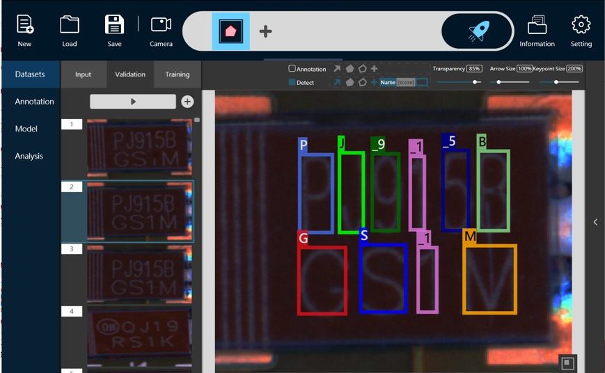
Overcoming traditional AOI limitations, Solomon’s SolVision quickly performs OCR without being affected by background or lighting conditions, complexity, or appearance of the serial number.
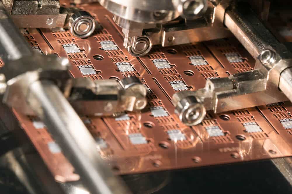
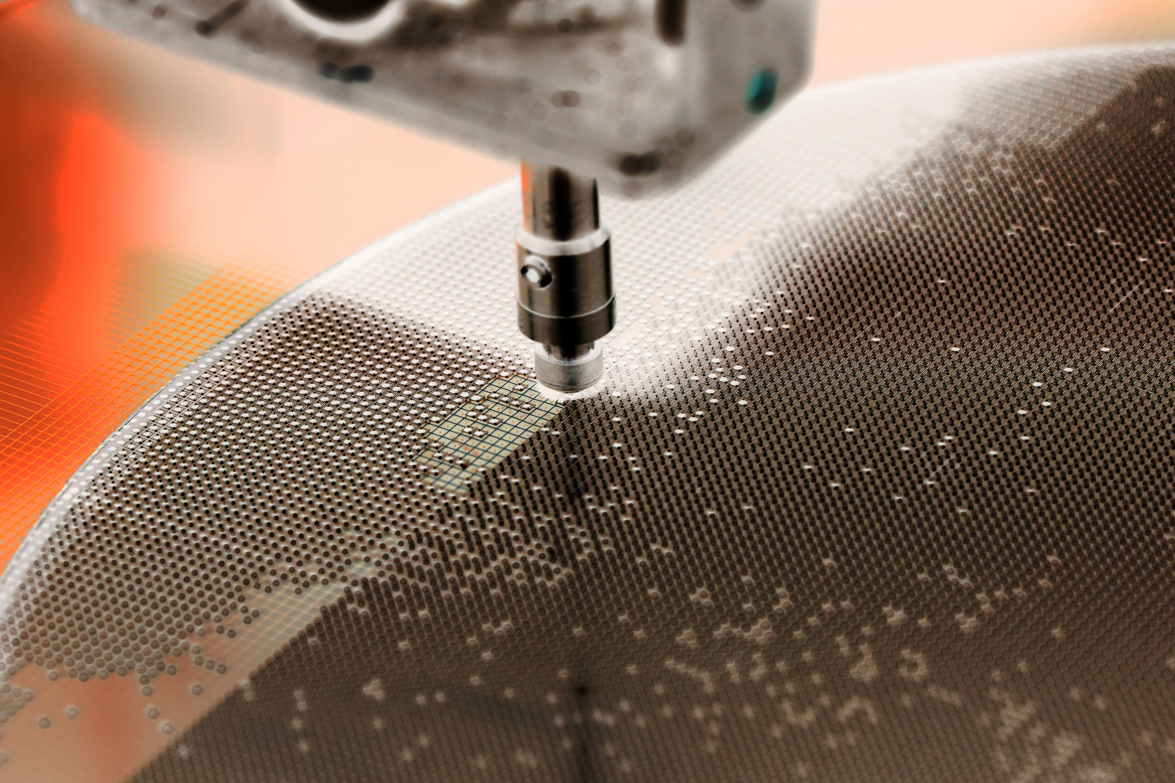
Excessive adhesive may remain on the chip or overflow on the circuit board and cause the chip to tilt, affecting stability of the whole semiconductor package.
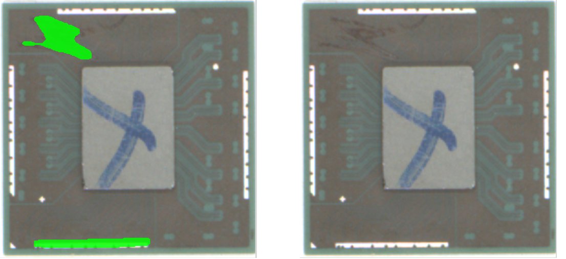
Faulty wafers also usually have subtle defects randomly scattered on the surface, and this prevents AOI systems from setting rules for efficient inspections.
SolVision enables visual inspection through AI image analysis, strengthening the reliability of displacement and angle information to recognize defective products and errors in the die bonding process.